Go Home
Go To Introduction
This is Book 1
Chapter 1 - Electricity
Chapter 1.2 - The Numbers
Chapter 2 - Sharing and Bonding
Chapter 3 - Voltage
Chapter 3.2 - Voltage Static
Chapter 3.3 - Batteries
Chapter 3.4 - Solar - Others
Chapter 4 - Resistance
Chapter 4.2 - Parallel Resistance
Chapter 4.3 - Voltage Dividers
Chapter 5 - Semiconductor
Chapter 5.2 - PNP NPN Junctions
Chapter 6 - Capacitor
Back To The Guide
To Book 2
The N-P-N and P-N-P Junctions
In this section we will look into two-junction devices, generally called
transistors. Transistors were developed in the late 1940's by researchers
in the Bell Telephone Laboratories. The discovery was based on earlier works
by Lilienfeld. The dual junction crystal structures of the transistor
provides the fundamental solid state architecture that allows flow-control
to be placed on the flow of electrons. When transistors came on the scene,
these three-legged devices provided the innovation that fueled a sweeping
change in electronic technology. They started replacing vacuum tubes
(Flimming valve) in the 1950's and early 1960's. No longer were we confined
to simple circuits taking up the space of a shoe box or two. The shoe box
could hold a large array of technology. Engineering started thinking about
electronic miniaturization. Before long, this technology gave way to
intergrading tens, then hundreds, then thousands, then millions of the NPN,
and PNP devices into a single wafer device.
In this section we will study transistors to understand how they work
and play together. Regardless of how powerful your computer, your
controller, your stereo, or your device is, eventually you may want to
output the results to do actual work, and that interface is based on the
theories of transistorized IO devices. Who knows, you might want to drive
a robot, build a sun tracking solar array, a DYI wind turbine for the
cabin, an HO train controller, or just make some yard art like a wooden
Owl with flashing eyes.
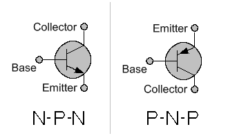
These are the schematic drawing symbols for the basic NPN and PNP transistors.
In both cases the emitter arrow is pointing toward the negative portion of
the circuit The named NPN and PNP are based on the construction materials,
thus the way each is placed into a circuit. The three legs of the transistor
are called the Emitter, Base, and Collector. The base lead is the control
lead in the transistor circuit. What that means is that it takes very little
change in base current (emitter-base current) to cause a large change in the
current flowing between the Emitter-Collector junction. The base is an
"electron" valve or gate that manages how many electrons flow through the
transistor at a time.
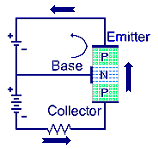
The NPN Circuit
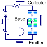
1. Quick look at the NPN transistor
2. When there is no base current flowing in the
emitter-base junction, the circuit is off.
3. With a small emitter-base potential (0.7 V)
the current starts to flow from the emitter
to the base and the transistor turns on.
4. Activating the base current reduces the
emitter-collector junction barrier and
emitter-collector current starts to flow.
5. Small change in base current gives large
change in collector current.
Controlling an LED with an NPN Transistor
Experiment with the NPN transistor and an LED:
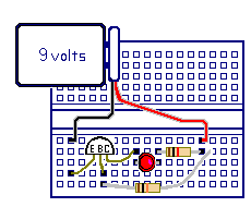
Review the Resistor Color Code chart and wire up the kit as described.
Perform the lab, and record your results.
Parts List:
1 9-volt battery
1 Battery power clip
1 2n3904 transistor - Q1
1 1 k ohm resistor - R1
1 100 k ohm resistor - R2
1 red light emitting diode
1 experimenters board
Miscellaneous:
hookup wire
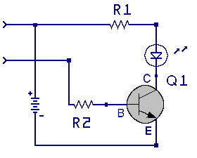
In this experiment we will be using a 2n3904 NPN transistor to control
the power for a light emitting diode (LED). By touching the loose end
of R2, the 100K resistor, to the V+ side of the 9V battery, the
transistor emitter-base junction will be activated. This will turn on
the emitter-collector junction and current will start to flow through
the transistor and LED. The LED will start emitting photon energy.
The PNP Circuit
1. Quick look at the PNP transistor circuit.
2. The same basic rules apply, however the PNP
sits in the circuit as a complement to the NPN.
3. When there is no base current flowing in the
emitter-base junction, the circuit in off.
Please Note: The emitter is tied to the more
positive portion of the circuit.
3. Lowering the emitter-base potential (0.7 V),
starts current flowing in the emitter-base
junction, turning on the transistor.
4. Activating the base current reduces the emitter-collector junction
barrier and emitter-collector current starts to flow.
5. Small change in base current gives large change in collector current.
The Push Pull Power Amplifier:
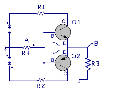
OK, If all is clear to this point, it is time to place both transistors
into a common circuit.
In this circuit the output voltage at B follow the
input voltage A with respect to common ground. We
will see that a small change at Test Point A, will give a larger change
at test point B. This circuit is a current amplifier.
There is a negative power supply and a positive power supply voltage with
respect to ground (0 Volts). Both the input and output voltage can go
through the 0 voltage point both in a positive and in a negative direction.
For this example, consider the junction voltages for both transistors to be
about 0.7 volts, resistors R1, R2, and R3 are 1K and R4 is 10K, and both
batteries are about 5 volts.
At the start, consider the voltage at Test Point A to be 0 volts. This means
both transistor base voltages are 0 volts. Test Point B is also at 0 V, and
no current is flowing through R3. NOTE: R3 is tied between power supply
common (0 V) and Test Point B.
With both Q1 and Q2 off the collector of Q1 is +5 volts and the collector of Q2 is -5 volts.
Hang on, because here we go!
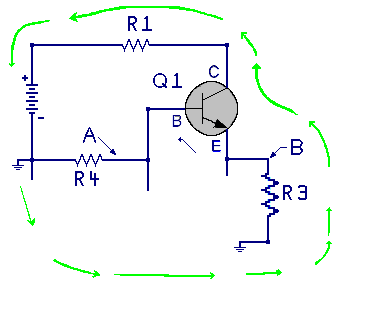
We will provide an external potential and adjust Test Point A of +2.0V.
Just at that moment, transition Q1 will see its Emitter-Base (E-B) voltage
attempt to raise. Q1 will react, wanting to keep this junction voltage at a
proper level (around 0.7 V). To do this it will turn on and allowing current
to flow, creating a voltage drop across R3 suitable enough to restore the
Q1 junction voltage back to the desired point. Q1 will also have emitter
to collector current flowing. At the same time Q2 will not see any need to
turn on, so its E-B junction will be off (Q2 will be acting as an insulator).
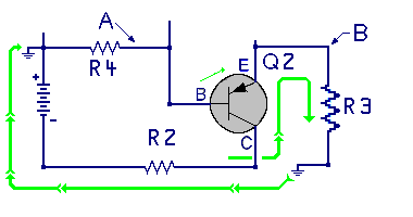
When Test Point A is set to -2.0V then Q2 will see the change in its
Emitter-Base (E-B) voltage and attempt to correct the junction voltage back to
about negative 0.7 V. In a PNP the Emitter it the most positive
voltage. At the same time Q1 will shut off and not see any need to turn on so its where
it E-B junction will be off (Q1 will be acting as an insulator). Now Q1 will
have no current flowing and Q2 will have emitter to collector current flowing. In the Q2
circuit the ground or 0 voltage level is the highest voltage in the circuit
and the battery is providing a -5 volt supply to the circuit.
The basic output voltage swing is about +1.3 volts to -1.3 volts.
If the values of R1, R2 and R3 were reduced in resistance the circuit would work
about the same but would drive more current through the load resistor R3.
This push-pull amplifier arrangement called emitter-follower which means
the emitter for each transistor follows its base. The current amplification
function for push-pull circuits is to supply power to its output over that
of signal amplification.
Many times a signal amplifier will be needed to front-end and drive a
Push-Pull amplifier being a power amplifier takes a small amount of power
at its input and provides a larger amount of power at its output.
« Previous Chapter Next Chapter »
Email us: info@shoeboxkits.com

