Chapter 5 - Introduction To Semiconductors

Go Home
Go To Introduction
This is Book 1
Chapter 1 - Electricity
Chapter 1.2 - The Numbers
Chapter 2 - Sharing and Bonding
Chapter 3 - Voltage
Chapter 3.2 - Voltage Static
Chapter 3.3 - Batteries
Chapter 3.4 - Solar - Others
Chapter 4 - Resistance
Chapter 4.2 - Parallel Resistance
Chapter 4.3 - Voltage Dividers
Chapter 5 - Semiconductor
Chapter 5.2 - PNP NPN Junctions
Chapter 6 - Capacitor
Back To The Guide
To Book 2
Introduction To Semiconductors
The semiconductor is a device with characteristics that lay between
those of a conductor and those of an insulator. What makes this
significant is the ability for the device to pass electrons/holes
under one set of circumstances and block the flow under different
circumstances. The semiconductor is at the heart of modern electronics.
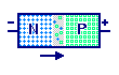
The semiconductor is based on the atomic and crystal structure called the
P-N Junction. The P-N junction is the basic building block used in making
electronic components including diodes, transistors, and integrated circuits,
microprocessors, memory chips, photovoltaic cells and so on. It is the
unique atomic bonding characteristics and the technologies used to build the
P-N Junction that made so many different configurations possible.
Although there are different processes for building the PN Junction, the
basic concepts are a layered approach. The process starts by growing a
crystal cylinder out of a material such as pure Silicon or Germanium. At
the atomic level, either material will provide room in the valiance shell
for 4 additional electrons. Once a crystal cylinder is grown in the lab it
is sliced into wafers.
Next, each silicon wafer is placed into a special oven where silicon oxide
layer forms on the surface of the wafer. Then each wafer undergoes a
photographic process and then an etch process to the oxide layer, leaving
a silicon oxide lattes pattern on the wafers surface.The process includes
adding a p-type and an n-type dopant to build a layered junction pattern.
Common p-type dopant impurities might be boron or gallium, each element with
3 electrons per atom in its valence shell. When applied, the bolding will
leave the lattes in a condition with one missing electron at each bonding
area. This is a "hole". The common p-type impurity material is called an
accepter material. This is because the bond process creates a hole waiting
to accept an electron.
Common N-type doping materials include phosphorus and arsenic, each with 5
electrons. Five electrons is one more than can nicely bond in the valance
shell. This extra electron will weakly bond, so it is easy to knock free
when a small potential is added. It is considered a free electron.
Another dopant is Indium. Can you check out its valance electrons, from
an online source, to determine whether it is of type N or type P?
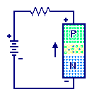
Forward bias of the Junction
Forward bias means that a voltage is applied in the direction that
commonly will allow electrons to flow.
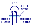
How does a Diode work?
In the circuit, an electrical potential is places on the diode in the
Forward bias direction. The negative terminal of the supply is connected
to the diode terminal connecting to the n-type material, also called the
Cathode, and the positive supply terminal is connected to the diode
terminal connecting to the p-type side, also called the Anode.
The Junction Region is where the P and N materials come together in the
lattes structure. This junction holds extra electron/hole sets waiting for
a Forward bias potential to be connected. A diode (P-N Junction) is a one-way
device allowing current to flow in the forward direction. Once that forward
potential exists, the electron/hole exchange process starts working. With
forward bias current on the junction, the semiconductor acts like a conductor.
NOTE: The voltage drop across the Silicon Junction is approximately 0.7 volt
of potential to overcome the internal barrier to start the current flowing
in the forward direction.
Reverse bias of the junction
When the positive side of the supply is connected to the n-type
material, the free electrons in the n-material are attracted to the
positive terminal and move away from the junction region. Likewise
the negative side of the supply attracts the p-material holes so they
also are not available at the junction region. The P-N Junction can
not exchange electron/hole sets, so practically no current flows,
making the semiconductor act as an insulator. There are a few
millionths of an amp (microamp) of current called leakage current
through the junction in the reverse direction. This is generally to
low to be of much interest most of the time.
There are two different situations when the reverse voltage becomes
large enough, that the junction properties will break down and the
junction will conduct electricity in the reverse direction across the
region. In the undesirable case, a situation called avalanche
breakdown, occurs because the reverse voltage is higher than the
junctions ability to block it. In the desirable case a special diode
called a zener diode is designed with a specifically engineered
breakdown voltage. There are special circuit designs that can benefit
from this special zener function. This property is called the zener
breakdown. Both avalanche and zener breakdowns will be discussed later
in the material.
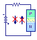
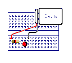
Going To The Work Bench
Experiment - Forward bias Diode
NOTE: Do not leave this circuit connected for an extended period of time as it will discharge the battery.
Go to the work bench.
Build this experiment, following the instructions that accompany the
kit. Review the Resistor Color Code chart and wire up the kit as
described. Perform the lab, and record your results.
Parts List:
1 9-volt battery
1 Battery power clip
1 1 k ohm resistor
1 red light emitting diode (flat side
toward battery black lead)
1 experimenters board
wire as needed
In this experiment we will be powering a light emitting diode (LED).
When current flows in the forward direction through an LED, the junction
emits a stream of photon energy. In this experiment the low energy is within
the visible range of light energy.
« Previous Chapter Next Chapter »
Email us: info@shoeboxkits.com