Chapter 12 - The Logic Of It All

This is Book 2
Chapter 7 - AC and Hertz
Chapter 8 - Magnetism
Chapter 8.2 - Inductors
Chapter 9 - Power Supply
Chapter 9.2 - Power Supply Filters
Chapter 10 - IC's and Amplifier
Chapter 10.2 - OP AMP Feedback and Unity Gain
Chapter 10.3 - OP AMP Non-Inverting
Chapter 10.4 - OP AMP Inverting
Chapter 11 - 555 Timer
Chapter 11.2 - Counters
Chapter 12 - Logic
Back To The Guide
Take Me Home
Logic - one step at a time
In this section we will take a look onto logic. More specifically digital
logic using 1's and 0's or binary logic using Boolean algebra. Logic
circuits have been with us for many years. These circuits can be build
using a number of devices from pneumatic and hydraulic valves to relays,
transistors and integrated circuits. We will start our investigation
using the common transistor.
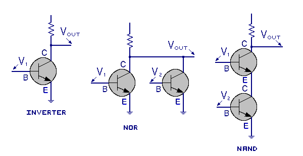
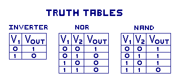
Here are some basic building blocks using transistorized circuits as
logic circuits. The first is the INVERTER. The inverter is a simple circuit
that gives an output opposite its input. So with the inverter, when its
input is moved from logic level of "0" (zero volts) to "1" (V+ volts) the
output responds by switching form level "1" to level "0". Remember in binary
digital logic we are only considering two levels of operation, either we
have the voltage or we have zero voltage. Think of the common light
switches used in houses.
They are either on or off. These are binary devices. The same holds true
with all binary logic devices. Binary devices are generally ON or OFF, 1's
or 0's, high or low, true or false. In this section we will be using "1's"
and "0's" to represent the voltage levels of the inputs and outputs. In the
NOR circuit (not or), the output moves from 1 to 0 when V1 or V2 or both V1
and V2 move from 0 to 1. In the NAND circuit (not and) the results are the
output moving from 1 to 0 when both V1 and V2 move from 0 to 1. If there
were three or more inputs they would all have to move to get the output to move.
These are simple views and the actual circuitry is much more sophisticated.
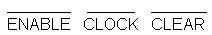
The NOT or Bubble operators
The Bubble is a circle or large period at the beginning or end of a
logic circuit. It represents a switch in logic, both in the words used
and in the voltage level. How this works will become clearer in the next
examples. The three circuits above all use the bubble to describe the
output as being opposite the input action. The Bubble is the "NOT" or "N"
part of the circuit name. Some devices with the Bubble have names like
NOR and NAND, and some devices without the Bubble are OR and AND, both of
which we will study in the next few examples.
The NOT operator can also be written with a line or bar atop the word and
read as: "NOT ENABLE", "NOT CLOCK" and "NO CLEAR". This might tell the
designer to use a logical "0" to perform actions such as to, ENABLE a
circuit, trigger a CLOCK pulse, or CLEAR a counter, for example.
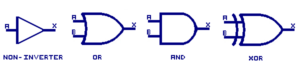
The Logic Of It All
There are seven common logic building blocks used to make up a sizable
portion of the electronic digital logic field. We have just looked at
three of these in the transistorized models section. Again these are the
INVERTER, the NOR GATE and the NAND GATE. We will now take a look at the
three complement devices to the above mentioned ones, and one special
case device.
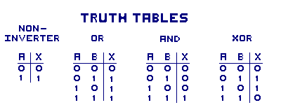
This graphic shows the schematic symbols for the logic functions of the
NON-INVERTER, the OR gate, the AND gate and the EXCLUSIVE OR gate. These
gate devices are drawn as two-input devices. Gates can have three, or
more inputs, however their operations are the same.
Looking at the Truth Table for the NON-INVERTER (also called BUFFER)
device we see that the input and the output are the same. When input
"A" is "0", the output "X" is "0", and when the input is 1 the output
is 1. In effect a Buffer is two invertors, in series.
From the second truth table, the table represents a two input OR gate.
When any number or all inputs at level 1 the OR gate will produce an
output of level of 1.
The third truth table represents the AND gate. This gate requires all
inputs to be "1" for the output to be a 1. If the AND gate has 6
inputs, it would take Input 1 and 2 and 3 and 4 and 5 and 6 to all be
high, for an output of 1. Applying this idea to a house alarm system,
you might want all 6 windows closed to keep the burglar alarm in a silent
state. Any failure in the input circuits will trip the alarm.
The forth truth table is a little different. This is an EXCLUSIVE OR
gate. What that means is that the output is high just when only one input
is high, all other cases the output is low.
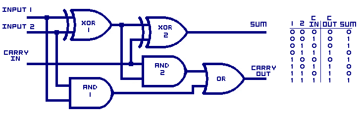
Binary Full Adder
This circuit is a binary full Adder. Recall form Chapter One, there was
a descussion about carry, where in the base with exponent 0's column
carried a number to the exponent 1's column. In the Full Adder circuit
there are three inputs, INPUT 1, INPUT 2 and CARRY IN, and there are
two outputs, the SUM and the CARRY OUT. Generally the CARRY IN is fed
from a previous stage and the CARRY OUT feeds another set of full adders.
Here is how the full adder works.
When just one input is "1" the SUM is "1" and CARRY OUT is "0".
With two inputs as "1" the SUM is "0" and the CARRY OUT is "1".
With three 1's as inputs the SUM is "1" and the CARRY OUT is "1".
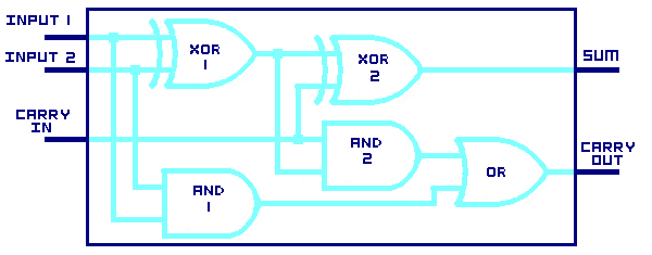
A Bit Of Black Box Magic
Recall that during the 555 IC section the 555 was represented as a Black
Box. Here is the black box Half Adder circuit. Because this book is not
about designing the actual components we will give our attention toward
how to use the components already on the market today. We only care about
the specification of any components from the Black Box perspective.
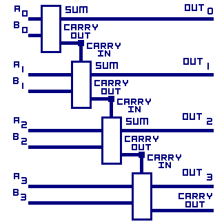
Here is a circuit putting together 4 Full Adders. This circuit will add
the two binary bits in exponent range 0 1 2 and 3 and give the correct
outputs. This is a hardware based 4-bit-set binary calculator and is
much faster then the same function build using a computer. You can also
easily expand this for additional bits. The disadvantage of a hardware
calculator is that this is all it can do.
Well this is the end of the second online book in this series. If you are
comfortable in applying what you have learned, you have gained much in the
fundamentals of electronics.
Just like in the first book, this book has an accompanying lab series that
can be purchased directly from Shoebox Kits. Each kit expands on the free
materials provided on this site.
« Previous Chapter Back To The Guide »
Email us: info@shoeboxkits.com